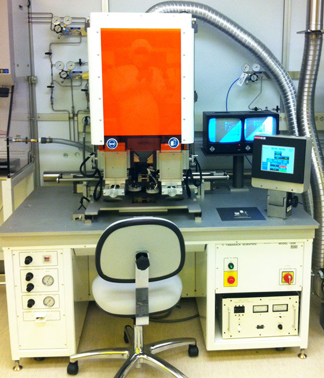
What is a Mask Aligner?
 A mask aligner is an instrument enabling photolithography (also called optical lithography),
which is a microfabrication process used to selectively remove parts of a thin film
to create a pattern or a design onto a substrate. To generate this pattern, the substrate
is first coated with a light-sensitive chemical (photoresist, or simply "resist").
(Coating of the substrate with a resist can be performed with the Laurell WS 650 Spin
Coater present at the IMC.) The substrate is then introduced into the mask aligner
and a mask with the desired pattern is placed above the substrate. A high intensity
ultraviolet light is shined over the mask. The light only transmits through the openings
in the pattern allowing the pattern to evaporate corresponding areas of the photoresist
layer of the substrate. Silicon wafers are common substrates and a commonly used resist
is polymethyl methacrylate (PMMA).
Mask aligners are widely used to generate integrated electronic circuits, specialty photonics materials and microfluidic channels.
Major Features and Specifications of the Tamarak 152
- Stand-alone, single sided, manual alignment and exposure system.
- Uses a photomask holder for glass and quartz
- Uses a substrate holder with stepper motors for X, Y, and Theta alignment
- Provides rapid and precise alignment of substrates with respect to photomasks
- Designed to accommodate wafers of 4" and 2" in diameter, 3" x 1"glass microscope slides, and 1cm x 1cm substrates
- Collimation half angle: < 3°
- Declination angle: < 2°
- Intensity: > 45 mW/cm² at broadband (350-450nm); > 25 mW/cm² at 365 nm
- Uniformity: <+ 6%
- Exposure wavelength from 350 nm to 450 nm, with intensity peaks at 365nm (i-line), 405nm (h-line), and 436nm (g-line)
Users interested in using the Materials Science Lab or equipment should contact:
